Project Overview
For my EGR 518 final project at Grand Valley State University, I designed and simulated a common-emitter RF amplifier around a BFP410 transistor at 2.4 GHz. The work covered transistor biasing, stability analysis, the tradeoff between gain and noise, and matching networks for a 50 Ω system. The final report was submitted on April 27, 2026.
This was a simulation project. I did not fabricate or test a physical amplifier. The figures below show calculations, circuit simulations, and a preliminary PCB layout; all performance values are simulated or calculated.
The goal was to amplify a small RF signal while keeping the transistor stable and choosing practical source and load impedances. At these frequencies, the connections and matching networks become part of the circuit design, so the project extended beyond choosing a transistor and setting its bias current.
Results at a Glance
The complete amplifier simulation produced useful gain at the target frequency, but the matching design still needed refinement before it could become a hardware design.
| Quantity | Result at 2.4 GHz |
|---|---|
| Forward transmission, S21 | Approximately 17.4 dB |
| Input reflection, S11 | Approximately −7.5 dB |
| Output reflection, S22 | Approximately −38 dB |
| Output impedance | Approximately 48.8 − j0.475 Ω |
| Group delay | Approximately 0.36 ns |
| Physical build or bench measurements | None; simulation only |
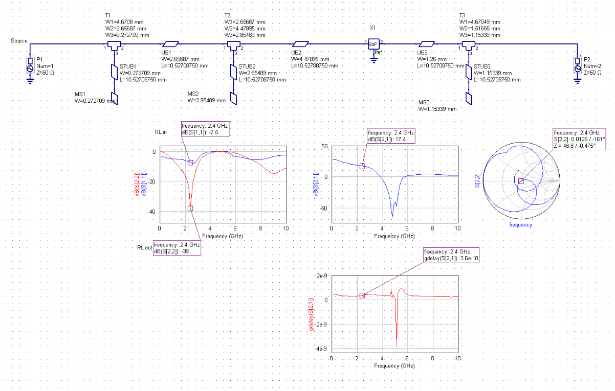
The response was broad rather than a distinct passband centered at 2.4 GHz. A suspected copy-and-paste error in the output matching calculations remained unresolved at submission. The gain and output match were encouraging, but they did not establish that the amplifier was fully optimized, ready to manufacture, or experimentally verified.
Design Workflow
I used Python and a Jupyter notebook for the calculations and Smith-chart plots, LTspice for DC bias simulation, and uSimmics for the RF matching networks and complete amplifier response. The RF calculations used the manufacturer’s BFP410 Touchstone S-parameter file.
The design progressed through four steps:
- Establish a DC operating point for the transistor.
- Use its S-parameters to examine stability and available gain at 2.4 GHz.
- Select source and load conditions that balance gain, noise, and stability.
- Design and simulate matching networks, then examine the combined amplifier response.
Transistor Biasing
The original assignment specified a BFU660F with a collector current of 10 mA and a collector-emitter voltage of 2 V. I selected a BFP410 and revised the bias circuit around a 3.3 V supply after examining the load line and available voltage swing.
The final schematic uses a grounded emitter, a 22 kΩ base-bias resistor, and a 122 Ω collector resistor. The collector resistor turns changes in collector current into changes in collector voltage. Choosing the operating point determines how far that voltage can move before the transistor approaches cutoff or saturation.
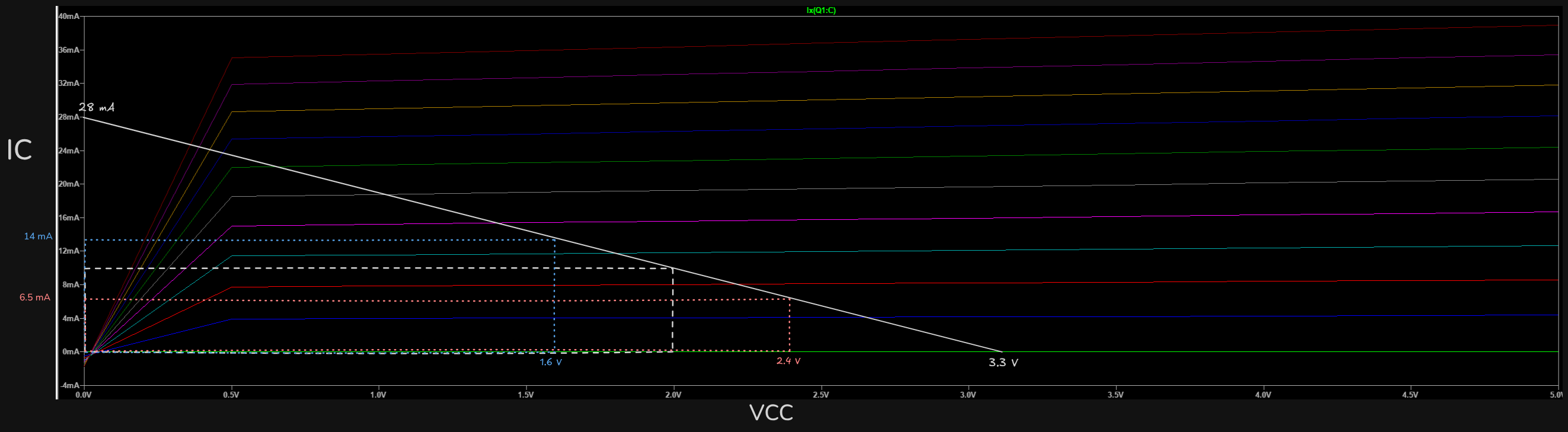
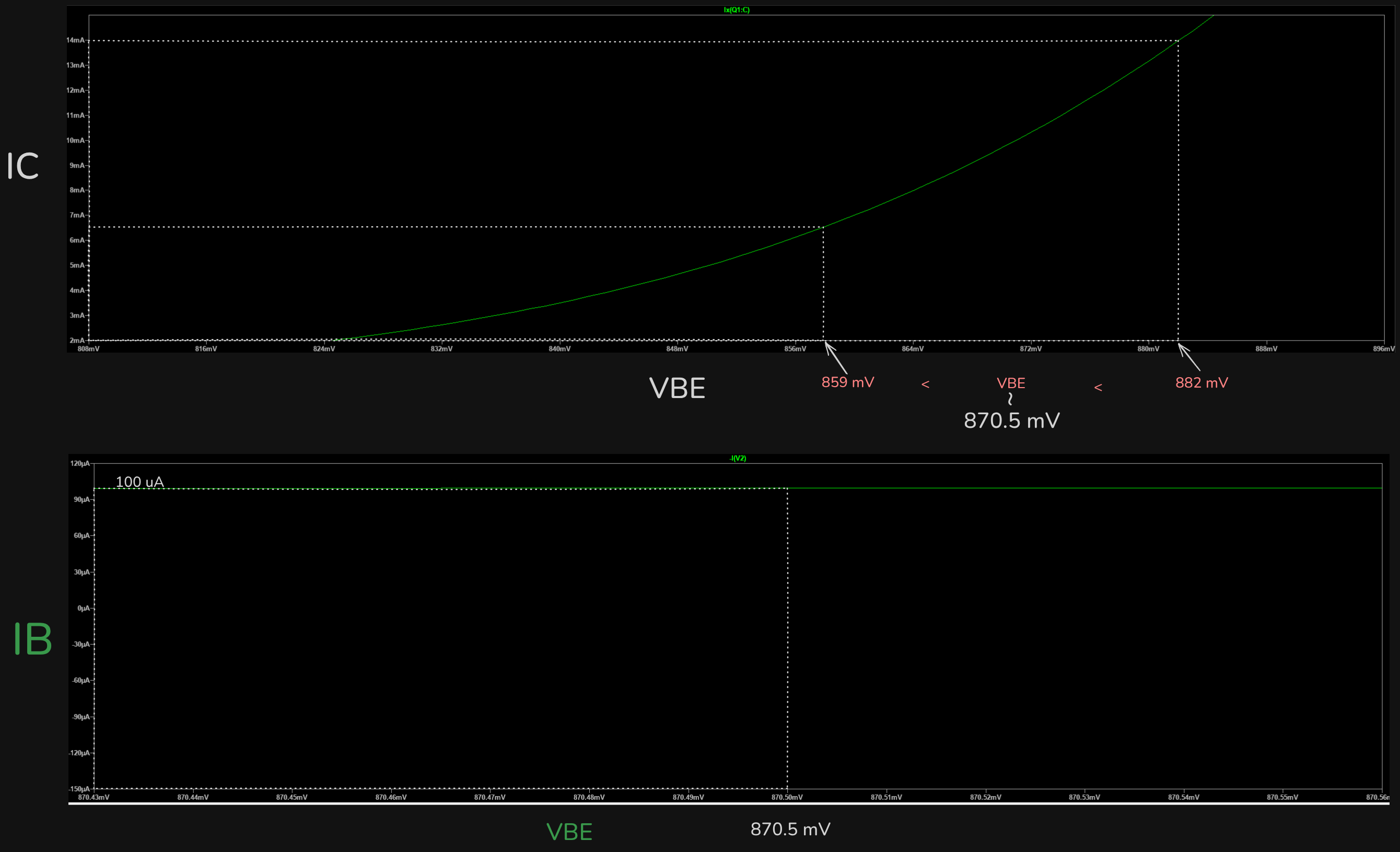
LTspice predicted a collector current of approximately 8.8 mA and a collector-emitter voltage of approximately 2.2 V. These were close to the intended 10 mA and 2 V, but not identical.
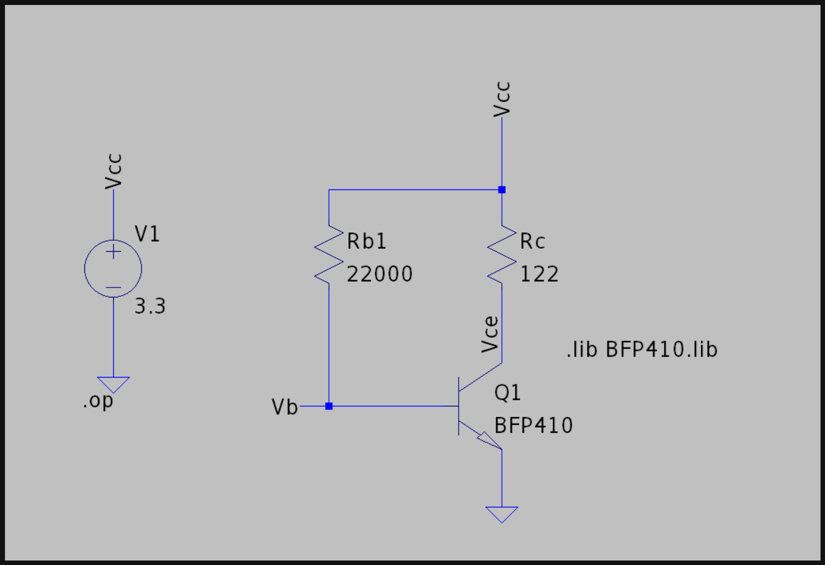
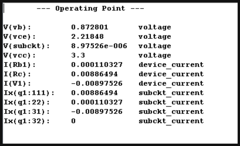
That difference matters because the RF S-parameter model was supplied for 10 mA and 2 V. The later RF results therefore describe that model’s operating point, rather than an exact characterization of the 8.8 mA, 2.2 V bias circuit. A further revision would bring the bias and RF model conditions into agreement.
Stability & Available Gain
S-parameters describe how incident and reflected waves relate at the transistor’s two ports. S11 and S22 describe reflections at the input and output; S21 describes forward transmission; S12 describes reverse transmission. The design calculations retained the reverse-transmission term instead of assuming a perfectly unilateral transistor.
For a two-port network, the Rollett stability factor is:
where
Using the archived model at 2.4 GHz gives approximately K = 1.00117 and |Δ| = 0.293. Together, K > 1 and |Δ| < 1 satisfy the unconditional-stability criterion at that frequency for the linear two-port model with passive source and load terminations.
K is only slightly above one. This single-frequency result is not evidence of stability across the entire frequency range or in a fabricated circuit with additional parasitics.
With those conditions satisfied, the calculated maximum available gain was approximately 19.6 dB:
The expression gives a linear power ratio; converting it to decibels gives the quoted value. It is an upper limit for the modeled device under the corresponding matching conditions, rather than the final amplifier’s simulated gain.
Choosing the Source & Load Conditions
Maximum gain was not the only design objective. I plotted input and output gain circles, stability circles, and a noise circle on a Smith chart to select a usable compromise.
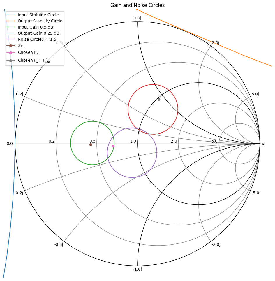
Each circle represents a set of reflection coefficients that satisfy a particular condition. The source selection affects both input matching and noise performance, so the best source impedance for low noise does not necessarily produce a perfect input match to 50 Ω.
The notebook’s selected source coefficient was approximately ΓS = −0.20 − j0.02. The corresponding load selection was approximately ΓL = 0.175 + j0.364. The notebook and final report contain different source-coefficient values; these values describe the saved notebook calculation, and the later simulation figures document the network results separately.
The report discusses input and output matching-gain circles of approximately 0.5 dB and 0.25 dB. Those are contributions associated with the matching conditions, not the total amplifier gain. The notebook calculated a transducer gain of approximately 17.37 dB for its selected source and load conditions.
The noise circle guided the design, but the preserved complete-amplifier results do not include a verified final noise-figure result.
Matching Network Design
The selected reflection coefficients were converted into impedances using a 50 Ω reference:
For the saved notebook selections, this gives a source impedance of approximately 33.3 − j1.39 Ω and a load impedance of approximately 51.5 + j44.7 Ω. The matching networks transform the external 50 Ω terminations into the impedances presented to the transistor.
I first developed lumped-element networks, then converted them to distributed transmission-line sections and stubs using Kuroda identities. The distributed simulations used microstrip on Rogers Duroid 5880. At 2.4 GHz, these line sections provide the required reactance through their electrical length and characteristic impedance.
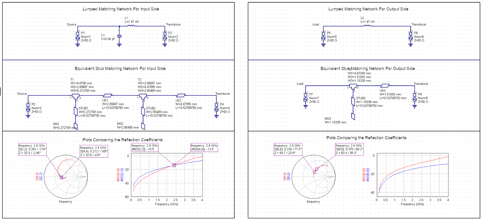
The input network approached its intended reflection coefficient. The output network differed from its intended target, and I later noticed a possible copy-and-paste error in the ΓL matching calculations. I did not resolve that issue before the deadline.
The complete amplifier’s low S22 at 2.4 GHz describes its output reflection relative to the external 50 Ω reference. It does not, by itself, prove that the internal load network reproduced the originally selected ΓL. Those are different checks, which is why the good output match does not erase the matching-network discrepancy.
What I Learned
- Bias and RF models need to agree. A nearby DC operating point is not automatically equivalent to the operating point used for the S-parameters.
- Gain, noise, and matching interact. Selecting an input condition for noise performance can mean accepting a less favorable 50 Ω input match.
- Verify each network before combining it. Checking the intended reflection coefficients helps catch mistakes that may otherwise survive into a plausible-looking final response.
- Keep calculated, simulated, and measured results distinct. This project produced a design study and simulation results, with no physical measurements.